BlackADC 820
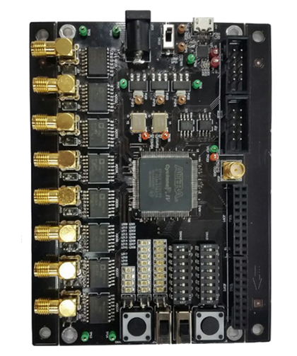
The BlackADC Board is FPGA based ADC board which can be configured to connect 16-Bit MCU, embedded system, or any digital system.
The board provides 8 channels AFE utilizing Analog Device AD7401 chip which can be configured up-to 20Mhz sampling frequency, accepting a differential input signal of ±250 mV (±320 mV full scale).
The AD7401A is offered in a 16-lead SOIC and has an operating temperature range of −40°C to +125°C.
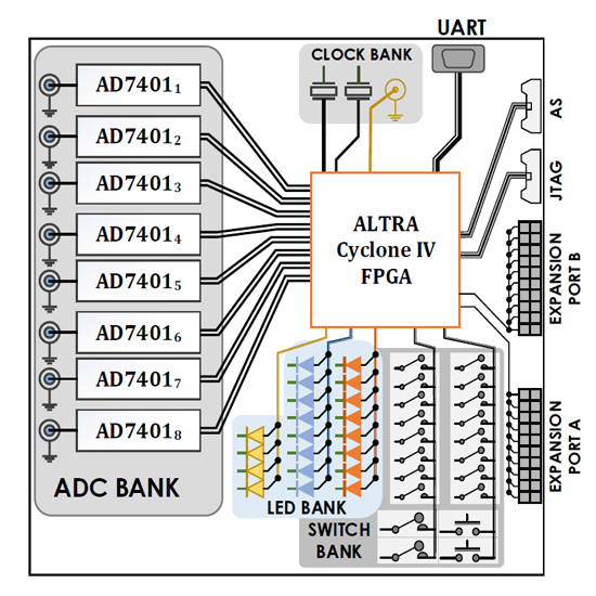
Eight AD7401 chips are directly connected to Altera Cyclone IV FPGA, so that all the channels can be sampled and data capturing can be done simultaneously.
The data so captured is stored in internal FPGA RAM and be acquired by 16-bit expansion port.
Powered with 5V DC supply makes it very low power consumption board.
제품설명
- Features:
-
Eight channel 16-bit 20MPS
Based on AD7401 connected FPGA in parallel
Input range differential input signal of ±250 mV
±320 mV full scale
Single ended AC or DC coupled analog input
Optional analog differential inputs
On board Cyclone IV EP4CE6E22 FPGA device
Coaxial front panel inputs for SSMC
On board switch, LED Array
Two sets of 20 pin expansion port
Compatible to Raspberry Pi.
Multiple clock setting:
Internal: 50Mhz and 27Mhz
External clock, connected to FPGA.
PC connectivity by Mini-UART port
JTAG and AS programmable port available for FPGA programming.
Many onboard test point
LPC (Low pin count) compatible
Noise shielding case – optional
No extra cooling required
 |
- Application
-
SONAR system
RADAR system
Medical equipment prototyping
Wireless communication receivers
High sampling test and measurement systems
- Support
-
User Guide
Reference Firmware design (VHDL)
Reference Altera Project for Cyclone series
Email support
- Product Includes:
-
1) BlackADC board
2) 5V DC adaptor
3) Altera Byte Blaster
4) Software CD:
a. FPGA programmable file
b. Software for data capturing on PC by UART
c. Drivers
d. Manual
e. Getting started: Tutorial
Typical Applications
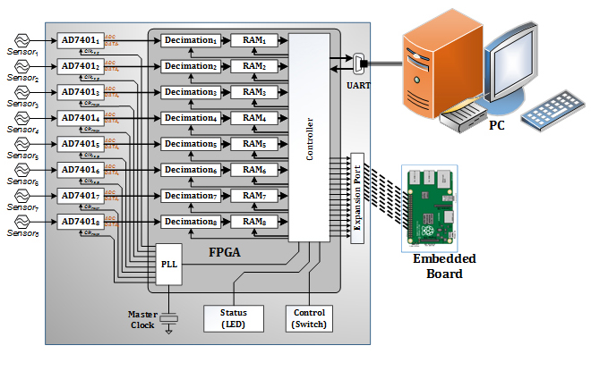
- Data Acquisition System
-
8 Sensors with different sampling frequency can be connected.
All sensor data can be captured in separate internal RAM.
On board LEDS can be used for status update for system.
On board switches can be used for hard control like panel.
Using UART interface, data can be received on PC.
Embedded board can be connected by expansion port for embedded platform.
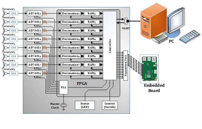
- Sonar/Radar Front-End receive
-
8 ultrasound transducer can be connected with suitable LNA interface to the board
The captured signal can be post processed on FPGA/Embedded board/PC
With on board FPGA and PLL, the frequency and phase of each transducer can be tuned easily.
- Prototyping Ultrasound System
-
The board can be connected with combin¬¬ation of analog multiplexer and switching circuit for prototyping complete ultrasound system
- Related Education Program:
-
DD 510 DD 520 DD 530 DD 540 Digital Design Techniques & Methodology Digital Design Techniques & Methodology Digital Design Techniques & Methodology Digital Design Techniques & Methodology VHDL for FPGA Design (I) VHDL for FPGA Design (II) VHDL for FPGA Design(III) VHDL for FPGA Design(IV) Beginners Introductory level Intermediate level Advanced Level Combinational and Sequential Logic Design for PLDs and ASICs,
Design and implement fundamental structures
Design and implement synchronous FSM
Designing with FPGA
VHDL concepts and constructs essential for FPGA design
Write VHDL for RTL synthesis
Targeting code to an FPGA device
Test benches
Tool flow from VHDL through simulation, synthesis and PnR
Overview of ASIC and FPGA including a survey of state of the art devices
Effective Design methodologies and flows
Advance concepts of hardware simulation and synthesis
Introduction to Hardware-Software Co-design
VHDL coding for complex FPGA and ASIC design
Sophisticated Test benches
Coding hierarchical designs using multiple VHDL design libraries
Writing re-usable, parameterisable VHDL